
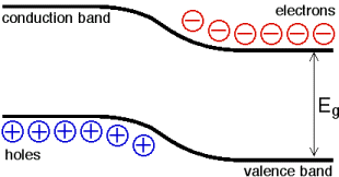
Note that such foam exhibits surface of both positive, both negative curvature. Electrons are repulsing mutually, so they're covering both surfaces of this sponge. The wet surface of sponge is responsible for good electrical and thermal conduction of common metals. At presence of hole conductivity the conductive electrons are collected inside of foam cavities preferably. The flat areas of zero curvature cannot keep the conductive electrons due the balance of electrostatic forces, and they correspond the band gap, occurring in common semiconductors. Under situation, when the motion of free electrons remains restricted to sponge cavities in continuous stripes arranged in hyperlattice, which are serving like pipes full of highly compressed electron gas, we can expect high temperature superconductivity in such system.
Another interesting situation may occur, when two pieces of sponge of different surface curvature are connected together. We can model such situation by connecting of two pieces of porous material, the hydrophilic and hydrophobic one, soaked by moderate amount of water. Because hydrophobic surface repels polar molecules of water, the water will collect inside of pores, thus emulating hole conductivity of P-type semiconductors. The hydrophilic material is attracted by water surface, so that water is forming bridges connecting convex surfaces and it represents a N-type of conductor here.

At the moment, when two pieces of such materials are connected together, the portion of fluid from hydrophobic material is soaked into the hydrophilic half of junction, thus removing water from cavities of neighboring part of hydrophobic material. This is a direct analogy of formation of space charge zone / depletion layer of semiconductor junction. Note that suction of liquid from hydrophilic part of junction doesn't improve the water transfer, it just leads to removal of additional amount of water from hydrophobic part, thus leaving it even less conductive for water molecules.

A quite different situation may appear, when we push additional amount of water in hydrophilic part. After soaking the dry portion of hydrophilic junction, the excessive water will fill up the cavities, so it can pass freely through capillary junction. Apparently, a surface tension based "diode" is formed, but we can imagine even much more complex structures analogous to transistor, thyristor and others, based on capillary forces inside of porous materials of different polarity. Nature supposedly uses these principles for controlled osmosis inside of living cells already, because surface of cell membranes is porous and it contains both hydrophilic, both hydrophobic part, formed by phospholipides.
Note that pushing of fluid into our "capillary diode" requires to overcome pressure exerted by capillary repulsion during filling of emptied cavities inside of hydrophobic part of junction. This corresponds the voltage drop in forward bias direction of semiconductor junctions. We can even met with analogy of recombination at the flat portion of porous surface, when water droplets are forced to overcame negative surface tension, so their surfaces are moving in accelerated way. At the case of liquids of extreme surface tension (like the mercury inside of porous glass), such area can even become the source of audible noise, thus mimicking the formation of photons at the recombination centers of PN junction nearly completelly. Such centers can be observed by Lorentz microscopy directly in thin layer of low temperature superconductors (compare the embedded animation bellow).


_(bjl).svg)
5 comments:
http://img177.imageshack.us/img177/4793/normalsciencevsfaithc.png
Zephir,
Amazing model, based on AWT, to explain the behaviour of the semiconductors without using Quantum Mechanics.
Thanks for the post.
Hi Cid..
Now we can compose fluid based analogies of electronic circuits, because we have all four fundamental components available.
The researchers observed a phenomenon they call flow rectification: an asymmetry in the flow rate with respect to voltage reversal. They found that when the voltage is reversed, the capillary sucks in fluid as expected, but at a much lower rate. The capillary thus behaves like a semiconductor diode — an electronic “valve” that allows current flow in only one direction — but with fluid flowing in place of electrons.
The Paradox Behind an Emerging Microfluidics Revolution Constructing switches out of pure liquid seemed impossible. Then researchers discovered Braess’ paradox could help. The team has found a way to control, switch or even reverse the flow in these corridors without any electronic control, which was deemed impossible so far.. If the H networks can act like switches, it’s not a huge stretch of the imagination to connect them together in a way that can perform logic operations.
Mechanical transistor utilizing only liquid is indeed possible and I also proposed one, based on dense aether model of semiconductors. I'm pretty sure it would work, because diode working on this principle has been published later and diode is the basis of every transistor. Except that my fluid switch utilizes surface tension instead of turbulence.
But the rectification device based on pure fluidic has been invented by Nicola Tesla already (so called Tesla valve). From this follows that the extension of this principle to pure fluidic switch shouldn't be so difficult after all - at least in principle. There exist fluidic vibrators, which work like astable oscillating circuit and the inertia of turbulent fluid serves as a inductance. If we collapse the oscillations by asymmetric flow we change astable oscillator to flip-flop circuit, the inductance of which would collapse, so that it may serve as a switch as well (the same effect will ruin induction heater once it stops oscillate). This is also the way in which Braess’ paradox. works: at certain range of pressures, the total flow through the H increased when the connecting corridor gets closed.
Post a Comment